Cost analysis tool for co-optimization of heterogeneous chiplets
Student: Alexander Graening
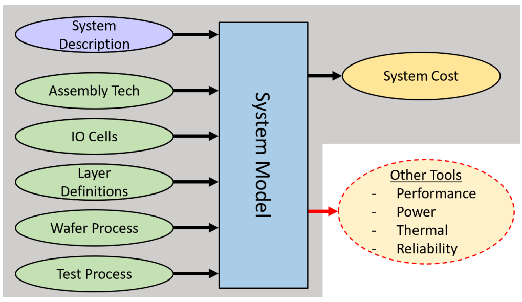
As chiplet-based systems become increasingly common in high-performance computing, design complexity has grown significantly. Rather than relying on a single die per package, designers now have various 3D integration options whether through vertical stacking or horizontal placement on a substrate with numerous configuration and process choices. In chiplet design, critical early decisions such as the number of chiplets, partitioning strategy, and interconnect type strongly impact overall performance and cost. In this work, we introduce CATCH, an open-source tool that supports these early design trade-offs. Through several case studies, we demonstrate how CATCH provides insights into optimal chip size, defect density, test and assembly cost, IO selection, and substrate choice, including a detailed cost breakdown based on prior research.
Thermal Performance Co-optimization
Students: Dedeepyo Ray, George Karfakis, Alexander Graening
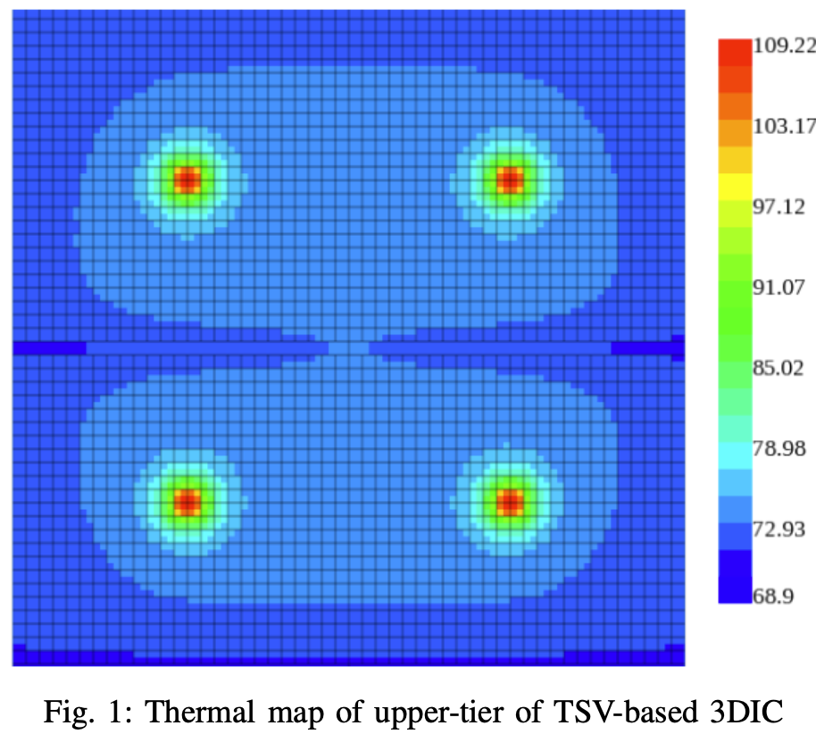
Modern workloads place heavy computational demands on hardware, increasing thermal stress and the need for robust cooling. While multi-die and chiplet systems with heterogeneous technologies and diverse stacking strategies help meet these demands, their thermal–performance interactions remain underexplored. Accurately capturing the cost implications requires a framework that co-optimizes performance and thermal behavior. In this work, we integrate temperature-induced performance throttling into existing performance and cost models to account for thermal effects and identify optimal operating points for system efficiency. Specifically, we extend CATCH, a chiplet cost-estimation tool, and DeepFlow, a performance modeling framework, to include thermal constraints and their impact on performance. We validate our approach across a range of systems, from 2.5D GPUs to complex 3D-stacked wafer-scale architectures.
Yield Modeling for Advanced Packaging
Students: Zhichao Chen, Jialong Chen, Alexander Graening, Jooyeon Jeong
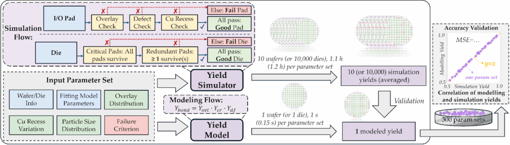
Among various approaches, Cu-Cu hybrid bonding has become a leading technique for high-density chiplet integration. This work presents a yield model, YAP, for wafer-to-wafer (W2W) and die-to-wafer (D2W) hybrid bonding. The model captures major yield loss mechanisms, including overlay misalignment, particle contamination, Cu recess variations, die/wafer warpage, surface roughness, and Cu density variations. This model enables co-optimization across packaging processes, design rules, and overall system methodology. Using this model, we analyze bonding pitch scaling, compare W2W and D2W bonding across chiplet sizes, and assess the benefits of tighter process control, such as reduced particle defects and higher alignment accuracy. Additionally, we demonstrate the impact of I/O pad layout on the bonding yield.
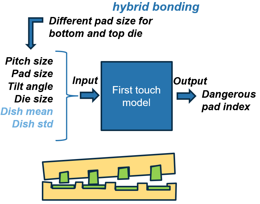
IO cell designs typically contain a driver and some electrostatic discharge (ESD) protection. For advanced bonding pitches, the size of the IO cell can easily be larger than the area required for a bonding pad, significantly limiting the use of advanced bonding pitches. In order to reduce the amount of ESD protection in IO cells for advanced packaging, we need to understand the ESD mechanisms that cause failures. Typically, ESD manufacturing controls will reduce the magnitude of ESD events that occur, but will not entirely eliminate the discharge during bonding. Based on the assumption that this ESD event will occur at a location determined by the first point of copper-copper contact during bonding, we have developed a tool to simulate the risk of ESD events at different locations on a die or wafer for different bonding parameters and die size.
Generating and Benchmarking 3DIC Design Descriptions for 3Dblox and CATCH
Students: Rohan Soni, Richard Chen, Alexander Graening, Jooyeon Jeong
Designing systems built from chiplets (tiny, modular chips) is currently complicated because there is no automated way to translate detailed physical data, like the industry-standard 3Dblox format, into parameters used by high-level cost analysis tools such as CATCH. To solve this, we introduce a validated, open-source tool that provides bidirectional translation between the CATCH and 3Dblox formats, establishing a crucial new workflow for designers. This new capability allows engineering teams to perform early-stage cost analysis of their designs within the CATCH framework, based on physical data from 3Dblox, thereby significantly reducing overall design time and expense.
Publications:
- Z. Chen and P. Gupta, “YAP+: Pad-Layout-Aware Yield Modeling and Simulation for Hybrid Bonding,” IEEE Transactions on Computer-Aided Design of Integrated Circuits and Systems (TCAD), 2026.
- A. Graening, J. Talukdar, S. Pal, K. Chakrabarty, and P. Gupta, “CATCH: a cost analysis tool for co-optimization of chiplet-based heterogeneous systems,” IEEE Transactions on Computer-Aided Design of Integrated Circuits and Systems (TCAD), 2025.
- Z. Chen and P. Gupta, “YAP: Yield Modeling and Simulation for Advanced Packaging,” in Proc. ACM/IEEE Design Automation Conference (DAC), 2025, p. 7